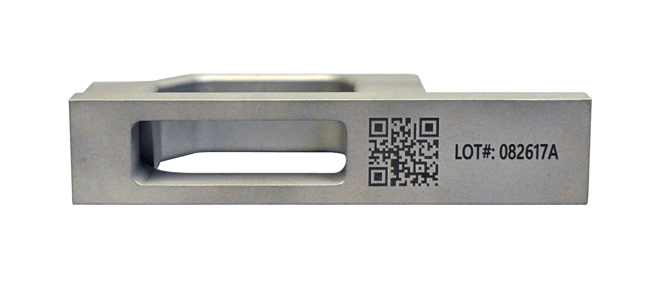
The laser marking of silicon wafers is an important part of the manufacturing process. The permanent mark on semiconductor packages is created with a concentrated light beam through a laser machine. The word laser isn’t just a regular word; it is an acronym that stands for “Light Amplification by Stimulated Emission of Radiation.” Light particles are focused and directed when an atom is stimulated to emit them. Wafers are laser marked in order to trace them throughout the manufacturing process with a laser marking machine, which can be programmed to precise specifications. The laser markings should be machine readable. Marking must also be finely detailed, since the mark can’t interfere with any processes on the underlying layer, and the wafer can’t be damaged in any way. Perfect use of laser for marking is required.
Silicon wafers – what are they?
Silicon wafers are marked with lasers to identify them, but what are they? All types of electronic devices contain wafers that function as semiconductors. A silicon wafer looks like a round disk with a mirrored surface. Since silicon wafers are impurity-free, they need to be handled with extreme care during laser marking.
The Process of Laser Marking
In order to mark silicon wafers, computer interaction is necessary. On a marking document, a map of the wafer is examined at this stage of the process. There are details about the parameters, functions, and other aspects of the wafer.
From the other side of the screen, you can see how your data will be translated into the silicon wafer. Once the settings are correct, you can place the wafer inside the laser marking machine. As the wafer is taken to the marking station, a mechanical hand will bring it there. It will be a completely automated process, with no need for human interaction. When the machine locates the target location, a laser beam will be shone on the water’s surface. After that process is complete, the completed project is transported to the receiving box, where it can be removed.
Several Advantages of Using Laser Marking

Accuracy
Laser marking is an excellent method for manufacturing wafers because of its precision. With its superior technology, even the smallest details are always completely accurate and detailed. For easy tracking, silicon wafers are marked with a few millimeters tall markings that can be read by computers.
High-Speed
The entire laser marking process is not only extremely precise, but also fast. From the time of placement, to the time of marking, to the time of completion, laser marking of a stack of silicon wafers can take place within minutes. Laser annealing provides an amazing finish without leaving anything behind on the surface, although it is a little slower than other marking methods.
Only the surface layer
Laser marking does not actually remove anything from the silicon surface. Only the color beneath the silicon surface changes. No damage is done to the silicon surface.
The effect is permanent
On silicon wafers, the markings are permanently etched. Whenever heat leaves a mark, it stays just below the surface, eliminating the possibility of it fading away.
A fully automated process
It is a fully automated system. The user does not need to interact with it. Silicon wafers can be picked up by a mechanical arm and transported within the machine to be marked by a mechanical arm. This results in laser marking machines being completely safe to use since the lasers will not interact with the wafer once they have changed the surface color. Furthermore, there will be fewer chances for costly mistakes to occur. By eliminating human error, there will be fewer chances for costly mistakes.
Environmentally safe
Since laser marking doesn’t use chemicals or inks, it is environmentally friendly compared to other methods of marking. The use of lasers also consumes very little energy, making them an excellent choice for marking silicon wafers.


